| CPC G06K 7/10316 (2013.01) [H01Q 1/2216 (2013.01); H01Q 7/00 (2013.01)] | 8 Claims |
|
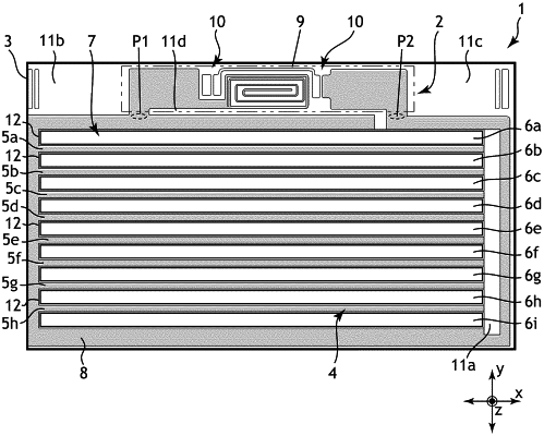
1. An antenna device which comprises an antenna structure constituted of a conductive material layer formed on a dielectric planar substrate and is configured to communicate with a radio frequency identification tag,
wherein the antenna structure comprises:
an active electrode group which comprises a plurality of striated active electrodes which extend in parallel with each other in a first direction, are kept in an electrically active state, and electrically connected with each other;
a passive electrode group which comprises a plurality of striated passive electrodes which extend in the same direction to sandwich the active electrode group therebetween, are formed to face each other, and not electrically connected with each other; and
a loop type plane electrode which connects the plurality of active electrodes to feeding points, and
an electromagnetic field is produced between the active electrodes and the passive electrodes by electromagnetic induction, an electromagnetic field which is different from the electromagnetic field in phase is produced between the loop type plane electrode and the passive electrodes by an electromagnetic mutual interference, and electromagnetic field density on the dielectric planar substrate is raised while forming magnetic fields with different phases within the same electromagnetic field.
|