| CPC G06F 7/5443 (2013.01) [G06F 7/50 (2013.01); G06F 7/523 (2013.01); H03K 19/20 (2013.01); H03M 1/466 (2013.01); H03M 1/68 (2013.01)] | 9 Claims |
|
1. A multiply-accumulate device, the device comprising:
a digital multiplication circuit, the digital multiplication circuit configured to input L m1-bit multipliers and L m2-bit multiplicands and configured to generate N one-bit multiplication outputs, each one-bit multiplication output corresponding to a result of a multiplication of one bit of one of the L m1-bit multipliers and one bit of one of the L m2-bit multiplicands;
a mixed signal adder, the mixed signal adder comprising:
one or more stages, at least one stage configured to input the N one-bit multiplication outputs, each stage comprising one or more inner product summation circuits; and
a digital reduction stage coupled to an output of a last stage of the one or more stages and configured to generate an output of the multiply-accumulate device based on the L m1-bit multipliers and the L m2-bit multiplicands,
wherein each inner product summation circuit comprises:
a controller configured to generate a digital output for the corresponding inner product summation circuit;
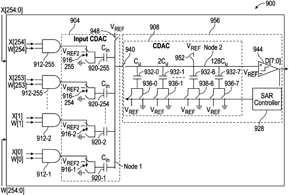
a common input node;
a plurality of capacitors, each of the plurality of capacitors having two terminals, one terminal of each capacitor being coupled to the common input node;
a precharge switch configured to selectively connect and isolate a reference voltage and the common input node;
a plurality of transmission gates, each transmission gate configured to charge a corresponding capacitor of the plurality of capacitors based on one of an output of a corresponding logic gate of a plurality of logic gates of the digital multiplication circuit and the digital output and to discharge the corresponding capacitor of the plurality of capacitors based on one of the output of the corresponding logic gate of the plurality of logic gates and the digital output;
a plurality of switch pairs, each switch pair being configured to couple a control input of a corresponding transmission gate of the plurality of transmission gates to one of the output of a corresponding logic gate of the plurality of logic gates and a corresponding bit of the digital output; and
a comparator configured to compare a voltage on the common input node and the reference voltage.
|