| CPC G06F 30/398 (2020.01) [H01L 21/321 (2013.01); H01L 29/401 (2013.01); G06F 2119/18 (2020.01)] | 26 Claims |
|
1. A process manufacturing method, comprising:
determining a type of to-be-formed MOS device and a corresponding threshold voltage interval;
obtaining, according to the MOS device type and the corresponding threshold voltage interval, a corresponding threshold voltage adjustment process by querying a pre-configured first mapping relationship of the threshold voltage interval and a second mapping relationship of the threshold voltage interval;
establishing a process flow according to the corresponding threshold voltage adjustment process, wherein:
the first mapping relationship is a mapping relationship between the threshold voltage interval and the MOS device type, and
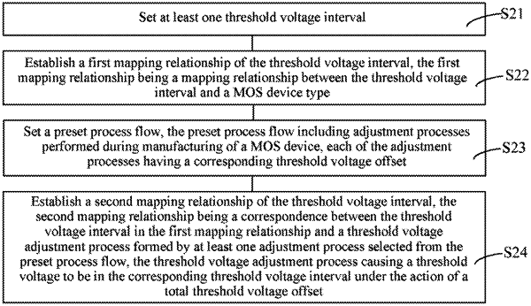
the second mapping relationship is a correspondence between the threshold voltage interval in the first mapping relationship and a threshold voltage adjustment process formed by at least one adjustment process selected from a preset process flow, the threshold voltage adjustment process causing a threshold voltage to be in the corresponding threshold voltage interval under the action of a total threshold voltage offset.
|