| CPC G06F 3/0655 (2013.01) [G06F 3/0671 (2013.01); G11C 7/1036 (2013.01); G11C 29/00 (2013.01)] | 21 Claims |
|
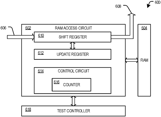
1. A circuit for reading or writing a random access memory (RAM), the circuit comprising:
a shift register coupled to the RAM, a test data input, and a test data output; and
a control circuit configured to generate a pulse every N clock cycles, each pulse triggering a RAM access operation transferring data between the shift register and the RAM, N being equal to a data width of the RAM divided by a parallel factor, the parallel factor being a number of pins in either the test data input or the test data output configured for parallel data loading.
|