| CPC G06F 3/0412 (2013.01) [G06F 3/0446 (2019.05); H10K 59/40 (2023.02); G06F 2203/04111 (2013.01); G06F 2203/04112 (2013.01)] | 16 Claims |
|
1. A display device, comprising:
a display panel having a base surface; and
an input sensor on the base surface,
wherein the input sensor comprises:
a first sensing electrode and a second sensing electrode, which are respectively extended in a first direction and a second direction crossing each other;
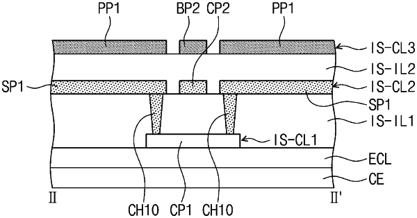
an insulating layer covering the first and second sensing electrodes; and
a first conductive pattern and a second conductive pattern, which are located on the insulating layer, are respectively overlapped with the first and second sensing electrodes, and are spaced from each other,
wherein the first sensing electrode comprises a plurality of first sensor units arranged along the first direction, and first connecting portions that connect adjacent ones of the first sensor units,
wherein the second sensing electrode comprises a plurality of second sensor units arranged along the second direction, and second connecting portions that connect adjacent ones of the second sensor units,
wherein the insulating layer comprises a first insulating layer and a second insulating layer,
wherein a group of connecting portions selected from the first connecting portions and the second connecting portions is on the base surface,
wherein the first insulating layer is on the selected group of the connecting portions,
wherein the first sensor units, the second sensor units, and another group of connecting portions, which are not selected from the first connecting portions and the second connecting portions, are on the first insulating layer,
wherein the second insulating layer is on the first sensor units, the second sensor units, and the another group of the connecting portions,
wherein the first and second conductive patterns are directly on the second insulating layer, and
wherein the second conductive pattern corresponds to a floating electrode and comprises:
a plurality of second floating portions overlapped with the second sensor units, respectively; and
a plurality of bridges connecting adjacent ones of the second floating portions.
|