| CPC G02B 6/14 (2013.01) [G02B 6/136 (2013.01); G02B 2006/12061 (2013.01); G02B 2006/12097 (2013.01); G02B 2006/12147 (2013.01); G02B 2006/12152 (2013.01)] | 4 Claims |
|
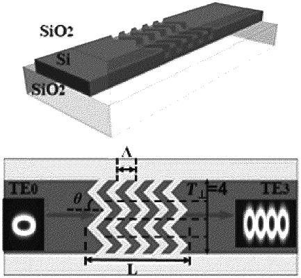
1. A compact silicon waveguide mode converter based on a dielectric meta-surface structure of periodical oblique sub-wavelength perturbations, the compact silicon waveguide mode converter comprising a top silicon structure with oblique subwavelength perturbations etched in certain cycles with periodical length of Λ, a duty cycle and an oblique angle θ on the Silicon-on-Insulator (SOI) substrate, Λ represents the cycle of the subwavelength structure; wherein
the top silicon structure with oblique subwavelength perturbations meets the mode coupling equation:
 wherein A and B are the amplitudes of modes A and B, and βa and βb show the propagation coefficients of the mode A and the mode B respectively; κab and κba represent the exchange coupling coefficient between waveguide modes a and b, namely the mode coupling coefficient, and κab=κba*; j represents the order of mode TEj; z represents the coordinate of the propagation direction;
wherein the mode coupling coefficient is further expressed as
 and Eb(x, y) represent the field distribution of waveguide modes a and b under the condition of no perturbation, ω represents the switch frequency, Δε(x, y, z) represents the change of dielectric constant corresponding to the cyclic perturbation, associating with etching shape; a represents the silicon waveguide length etched in one period divided by Λ.
|