| CPC G02B 6/132 (2013.01) [G02B 6/136 (2013.01); H04B 10/25 (2013.01); G02B 2006/12038 (2013.01); G02B 2006/12061 (2013.01); G02B 2006/12164 (2013.01)] | 20 Claims |
|
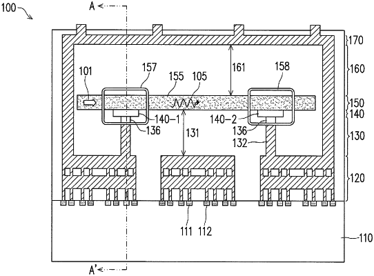
1. A photonic device, comprising:
a substrate;
a plurality of metal layers on the substrate;
a contact layer comprising a plurality of contacts over the plurality of metal layers;
a photonic material layer disposed on the contact layer; and
a waveguide on the photonic material layer, wherein
the photonic material layer comprises: a first photonic material sublayer, a first dielectric sublayer, a second photonic material sublayer, and a second dielectric sublayer, and
each of the first photonic material sublayer and the second photonic material sublayer is formed on and in contact with the contact layer.
|