| CPC G02B 6/122 (2013.01) [G02B 6/136 (2013.01); G02B 2006/12061 (2013.01)] | 20 Claims |
|
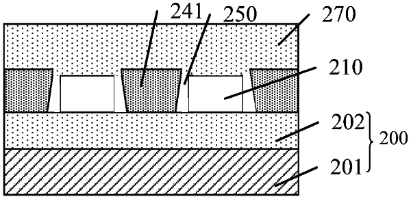
1. A semiconductor structure, comprising:
a base substrate;
an optical waveguide layer over the base substrate;
a first dielectric layer over the base substrate, wherein a cavity is formed between the first dielectric layer and the optical waveguide layer, and the cavity is located on sidewall surfaces of the optical waveguide layer and has a bottom coplanar with a bottom of the optical waveguide layer, and the cavity is filled with air; and
a second dielectric layer on the first dielectric layer and the optical waveguide layer, wherein the second dielectric layer is located on a top of the cavity and seals the cavity.
|