| CPC G02B 1/002 (2013.01) [G02B 5/005 (2013.01); G02B 5/1814 (2013.01); G02B 27/4211 (2013.01); B82Y 20/00 (2013.01)] | 18 Claims |
|
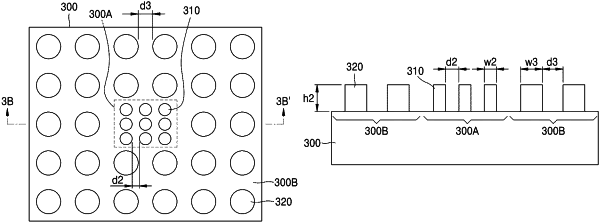
1. A meta-surface optical device comprising:
a transparent substrate;
a meta-surface comprising a plurality of first columnar patterns provided on a first region of an upper surface of the transparent substrate; and
a light control member comprising a plurality of second columnar patterns provided on a second region of the upper surface of the transparent substrate and configured to prevent light transmission,
wherein the plurality of first columnar patterns have a same height as the plurality of second columnar patterns and the plurality of second columnar patterns are configured to surround an entirety of the first region in which the meta-surface is provided, and
wherein the plurality of first columnar patterns and the plurality of second columnar patterns are made of a dielectric material.
|