| CPC G01R 31/2879 (2013.01) | 13 Claims |
|
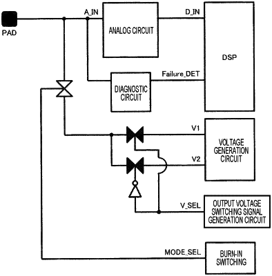
1. A semiconductor integrated circuit device comprising:
an analog circuit;
a diagnostic circuit that detects an abnormality on an input side of the analog circuit;
a digital signal processing unit connected to an analog circuit output side;
a voltage generation circuit that is connected to the input side of the analog circuit and generates a plurality of voltages; and
a switch circuit that is provided between the analog circuit and the voltage generation circuit and is switched on when a burn-in switching signal is input, wherein
the voltage generation circuit outputs a plurality of voltages that do not cause the diagnostic circuit to function.
|