| CPC G01R 15/207 (2013.01) [G01R 19/16571 (2013.01)] | 17 Claims |
|
1. A method of manufacturing a current sensor arrangement, the method comprising:
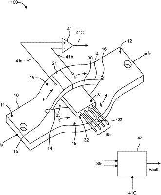
providing a first conductor piece that is configured to conduct a primary current, the first conductor piece comprising a first end and a second end oppositely arranged relative to the first end with respect to a current path of the primary current;
forming a first slit in the first conductor piece that extends partially from the first end towards the second end along the current path, wherein the first slit divides the first conductor piece into a first conductor portion and a second conductor portion both conjoined at the second end of the first conductor piece;
providing a second conductor piece that is configured to conduct the primary current, the second conductor piece comprising a third end and a fourth end oppositely arranged relative to the second end with respect to the current path of the primary current;
forming a second slit in the second conductor piece that extends partially from the third end towards the fourth end along the current path, wherein the second slit divides the second conductor piece into a third conductor portion and a fourth conductor portion both conjoined at the fourth end of the second conductor piece;
deforming the first conductor portion and the second conductor portion in opposite directions;
deforming the third conductor portion and the fourth conductor portion in opposite directions;
conjoining the first conductor portion and the third conductor portion via a first current impeding structure to form a first conjoined conductor structure;
conjoining the second conductor portion and the fourth conductor portion via a second current impeding structure to form a second conjoined conductor structure; and
inserting a magnetic sensor through a gap formed between the first conjoined conductor structure and the second conjoined conductor structure such that the first conjoined conductor structure is arranged over a first portion of the magnetic sensor and the second conjoined conductor structure is arranged under a second portion of the magnetic sensor.
|