| CPC G01L 1/22 (2013.01) [G02F 1/133512 (2013.01); G02F 1/136286 (2013.01); G03B 21/006 (2013.01); H01L 27/1214 (2013.01)] | 9 Claims |
|
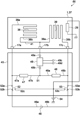
1. An electro-optical device, comprising:
an electro-optical panel including:
a first strain sensor element including a first resistance member and a second strain sensor element including a second resistance member that are provided in a pixel area; and
a first wiring electrically coupling the first strain sensor element and the second strain sensor element; and
a strain detection circuit including:
a first variable resistance member;
a second variable resistance member;
a second wiring electrically coupling the first variable resistance member and the second variable resistance member; and
a galvanometer electrically coupled to the first wiring and the second wiring,
wherein the first variable resistance member, the second resistance member and the galvanometer are provided in a circuit area different from the pixel area.
|