| CPC B81B 7/0035 (2013.01) [B81C 1/00277 (2013.01); B81C 2203/019 (2013.01); B81C 2203/0145 (2013.01)] | 20 Claims |
|
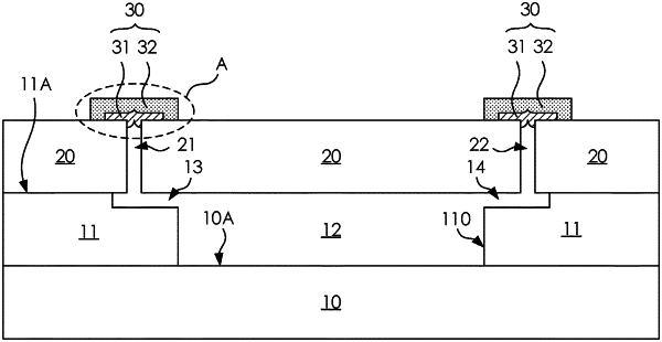
1. A semiconductor structure, comprising:
a first substrate;
a semiconductor layer over the first substrate, the semiconductor layer having a cavity at least partially through the semiconductor layer;
a second substrate over the semiconductor layer, the second substrate having a through hole; and
a eutectic sealing structure on the second substrate and covering the through hole;
wherein the eutectic sealing structure comprises a first metal layer and a second metal layer eutectically bonded on the first metal layer, and wherein the first metal layer has a protrusion at a top surface of the first metal layer.
|