| CPC B32B 17/1099 (2013.01) [B32B 17/10293 (2013.01); B32B 41/00 (2013.01); G01B 11/06 (2013.01); G01N 21/17 (2013.01); G01N 21/958 (2013.01); B32B 2041/04 (2013.01); B32B 2307/42 (2013.01); B32B 2457/20 (2013.01); G01N 2021/1765 (2013.01)] | 5 Claims |
|
1. A method of manufacturing a display device, the method comprising:
providing a glass including an edge region and an inner region;
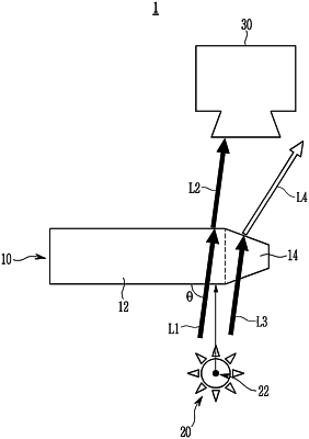
arranging a light source under the glass;
setting a center position of the light source to correspond to a first point of the glass;
directing light into the glass by using the light source;
first detecting a defect in the edge region of the glass by receiving light passing through the glass by using a detection camera;
adjusting the center position of the light source to correspond to a second point of the glass based on a quality of a result obtained by the first detecting; and
second detecting a defect in the edge region by using the light source with the adjusted center position to obtain a result having a quality different from that obtained by the first detecting.
|