| CPC B06B 1/0644 (2013.01) [B06B 1/0215 (2013.01); H10N 30/02 (2023.02); H10N 30/06 (2023.02); H10N 30/802 (2023.02); H10N 30/875 (2023.02); H10N 30/88 (2023.02)] | 4 Claims |
|
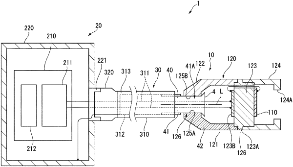
1. An ultrasonic device comprising:
an ultrasonic sensor;
a wiring member; and
a housing, wherein
the wiring member includes:
a signal line,
a covered wire that covers the signal line coupled to the ultrasonic sensor via an insulating layer, and
a conductive ring that is electrically coupled with the covered wire,
the signal line is inserted into the conductive ring,
the signal line is inserted into the housing through the conductive ring,
the housing covers the ultrasonic sensor and has a plurality of housing components having conductivity, and
the conductive ring is electrically coupled to and held by the plurality of housing components.
|