| CPC B06B 1/0622 (2013.01) [B06B 1/0611 (2013.01); G06V 40/1306 (2022.01); G06V 40/1329 (2022.01); H10N 30/02 (2023.02); H10N 30/06 (2023.02); H10N 30/072 (2023.02); H10N 30/082 (2023.02); H10N 30/1071 (2023.02); H10N 30/2047 (2023.02); H10N 30/875 (2023.02); H10N 30/883 (2023.02)] | 4 Claims |
|
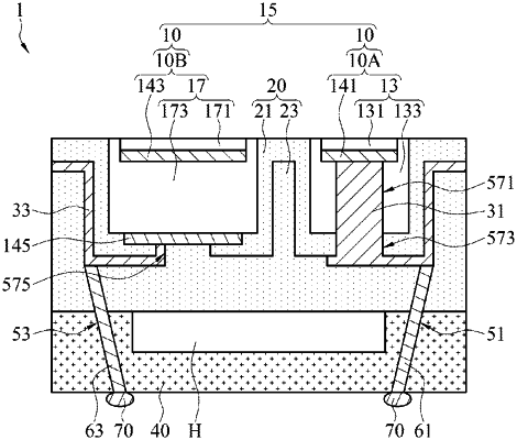
1. A manufacturing method of a wafer level ultrasonic device, comprising:
forming an ultrasonic element on a substrate, wherein the ultrasonic element comprises a first electrode and a second electrode that is not connected to the first electrode;
forming a first protective layer on the ultrasonic element and the substrate, and forming a first through hole and a second through hole that expose a part of the first electrode and a part of the second electrode;
forming a first conductive layer and a second conductive layer on the first protective layer, wherein a first conductive part of the first conductive layer is in the first through hole and is connected to the first electrode, and a second conductive part of the second conductive layer is in the second through hole and is connected to the second electrode;
forming a second protective layer on the ultrasonic element, the first protective layer, the first conductive layer, and the second conductive layer;
providing a base, and connecting the base and the second protective layer in a vacuum environment, wherein the base has an opening, and the opening forms a closed cavity with the protective layer;
removing the substrate;
forming a first electrical connection region and a second electrical connection region on the base, and forming a first groove and a second groove on the second protective layer, wherein the first groove and the second groove expose a first connection part of the first conductive layer and a second connection part of the second conductive layer respectively, and the first electrical connection region and the second electrical connection region are in communication with the first groove and the second groove respectively; and
filling the first electrical connection region, the second electrical connection region, the first groove, and the second groove with a metal material, so that the metal material is connected to the first conductive layer and the second conductive layer,
wherein the step of forming the ultrasonic element comprises:
forming a first piezoelectric material layer and a first electrode material layer on the substrate in sequence;
removing parts of the first piezoelectric material layer and the first electrode material layer, to form a first bottom piezoelectric layer and a second bottom piezoelectric layer that are separated from each other, and the first electrode and a second circuit layer that are separated from each other;
forming a second piezoelectric material layer and a second electrode material layer, wherein the second piezoelectric material layer covers the first bottom piezoelectric layer, the second bottom piezoelectric layer, the first electrode, and the second circuit layer; and
removing parts of the second piezoelectric material layer and the second electrode material layer, to form a first top piezoelectric layer, a second top piezoelectric layer, and the second electrode that are separated from each other, wherein the first top piezoelectric layer covers the first bottom piezoelectric layer and the first electrode, the second top piezoelectric layer covers the second bottom piezoelectric layer and the second circuit layer, and the second electrode is on the second top piezoelectric layer, to form a first ultrasonic unit and a second ultrasonic unit.
|