| CPC A61B 8/4488 (2013.01) [A61B 8/4494 (2013.01); A61B 8/463 (2013.01); A61B 8/5207 (2013.01); H01L 21/78 (2013.01); H10N 30/063 (2023.02); H10N 30/20 (2023.02); H10N 30/872 (2023.02); H10N 39/00 (2023.02); Y10T 29/42 (2015.01)] | 10 Claims |
|
1. A wafer scale method for manufacturing a grid of phased array transducers comprising:
providing a piezoelectric layer having a first side and a second side, wherein the piezoelectric layer comprises a piezoelectric material with a first metallized surface on the first side and second metallized surface on the second side, wherein the first metallized surface is directly applied to the piezoelectric material and the second metallized surface is directly applied to the piezoelectric material, wherein the first metallized surface forms a ground electrode and the second metallized surface forms a signal electrode;
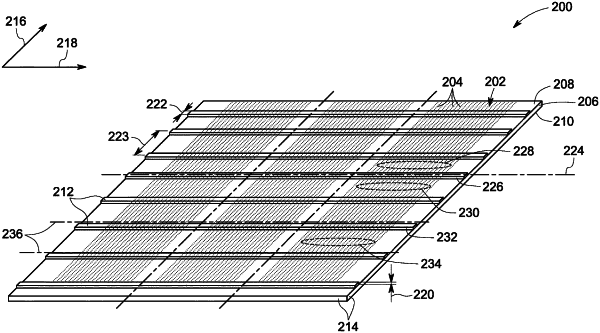
forming a plurality of ground contact traces along an elevational direction on the first side of the piezoelectric layer to define an acoustic array stack, wherein each of the plurality of ground contact traces is in electrical contact with the first metallized surface and extends along an azimuthal direction, wherein each of the plurality of ground contact traces has a width in the elevational direction that is less than 10% of a center-to-center distance between any two of the plurality of ground contact traces in the elevational direction;
dicing the acoustic array stack along the elevational direction perpendicular to the ground contact traces to define individual transducer elements that are electrically isolated from one another;
dicing the acoustic array stack along the azimuthal direction through the ground contact traces to define strips of phased array transducers such that at least a portion of each of the plurality of ground contact traces is exposed along a side of the strips of the phased array transducers;
coupling a carrier block to at least a portion of the acoustic array stack;
disposing a de-matching layer on the second side of the piezoelectric layer, wherein the de-matching layer is in contact with the metallized second surface; and
disposing one or more acoustic matching layers on the first side of the piezoelectric layer, wherein one of the one or more acoustic matching layers is in contact with both the plurality of ground contact traces and the first metallized surface.
|