| CPC H10K 59/131 (2023.02) [G09G 3/3233 (2013.01); G09G 3/3266 (2013.01); G09G 2300/0842 (2013.01); G09G 2310/0286 (2013.01); G11C 19/287 (2013.01); H01L 25/18 (2013.01)] | 20 Claims |
|
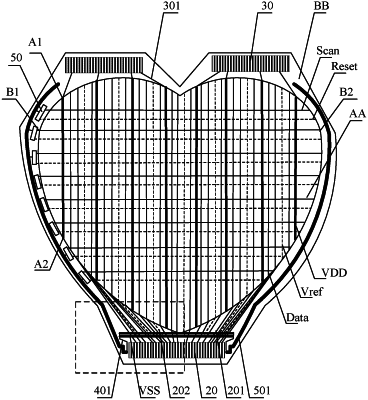
1. A display substrate, comprising a display region and a non-display region, wherein the display substrate comprises a base substrate, a driving structure layer and a wiring layer which are disposed on the base substrate; the driving structure layer is located in the display region, and the wiring layer is located in the non-display region; the driving structure layer comprises: a first power supply line, a data signal line and a reference signal line which extend along a first direction; the wiring layer comprises a first power supply wiring, a data wiring, and a reference wiring;
the first power supply wiring is electrically connected to the first power supply line, the data wiring is electrically connected to the data signal line, and the reference wiring is electrically connected to the reference signal line;
the first power supply wiring is located on a first side of the display region, and the data wiring is located on a second side of the display region, wherein the second side is different from the first side; the data wiring and the reference wiring are located on a same side of the display region;
for the first power supply line, the data signal line, and the reference signal line with a same length, a resistance of the first power supply line is greater than that of the data signal line and greater than that of the reference signal line.
|