| CPC H10K 50/852 (2023.02) [H10K 59/12 (2023.02); H10K 2102/351 (2023.02)] | 19 Claims |
|
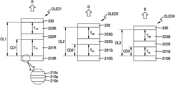
1. An organic light-emitting display apparatus, comprising:
a first pixel electrode, a second pixel electrode, and a third pixel electrode;
an opposite electrode disposed on the first pixel electrode, the second pixel electrode, and the third pixel electrode, and the opposite electrode facing the first pixel electrode, the second pixel electrode and the third pixel electrode;
a first organic emission layer disposed for emitting a first color, the first organic emission layer between the first pixel electrode and the opposite electrode;
a second organic emission layer for emitting a second color, the second organic emission layer disposed between the second pixel electrode and the opposite electrode;
a third organic emission layer for emitting a third color, the third organic emission layer disposed between the third pixel electrode and the opposite electrode;
a first lower functional layer disposed between the first pixel electrode and the first organic emission layer;
a second lower functional layer disposed between the second electrode and the second organic emission layer;
a third lower functional layer disposed between the third pixel electrode and the third organic emission layer;
a first upper functional layer disposed between the first organic emission layer and the opposite electrode;
a second upper functional layer disposed between the second organic emission layer and the opposite electrode;
a third upper functional layer disposed between the third organic emission layer and the opposite electrode, wherein
a thickness of each of the first upper functional layer, the second upper functional layer and the third functional layer is equal to or greater than 1300 Å and less than or equal to 1800 Å, and
a ratio of a thickness of the first upper functional layer to a thickness of the first lower functional layer is different from a ratio of a thickness of the second upper functional layer to a thickness of the second lower functional layer.
|