| CPC H05K 1/0219 (2013.01) [H05K 1/0215 (2013.01); H05K 2201/0707 (2013.01); H05K 2201/10409 (2013.01)] | 15 Claims |
|
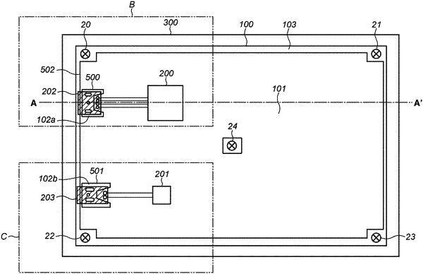
1. A printed circuit board comprising a conductor layer designed on one side of one substrate layer including:
a first ground region on which a connector to be connected with an external apparatus or communication cable is mounted and which is connected with a ground; and
a second ground region separated from the first ground region at the conductor layer, the second ground region being at a position that is outside the first ground region at least in a region corresponding to an opening of the connector on the conductor layer, and connected with a ground,
wherein the opening is an insertion opening of the connector into which the external apparatus or the communication cable are to be inserted.
|