| CPC H04L 7/0338 (2013.01) [H03L 7/091 (2013.01); H03L 7/0998 (2013.01)] | 20 Claims |
|
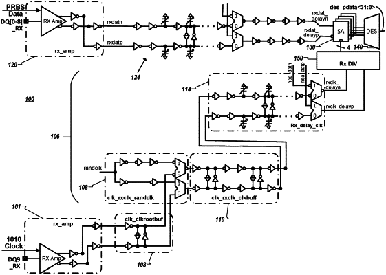
1. A device comprising:
feed-forward clock circuitry to provide a receiver (RX) clock to a sampler circuit and comprising a first plurality of inverters that cause a temperature-induced delay; and
an RX phase-locked loop (PLL) coupled between the feed-forward clock circuitry and the sampler circuit, the RX PLL comprising a second plurality of inverters having a negative delay that matches the temperature-induced delay of the first plurality of inverters.
|