| CPC H03K 17/168 (2013.01) [H03K 17/08 (2013.01); H03K 17/567 (2013.01); H03K 2017/0806 (2013.01)] | 15 Claims |
|
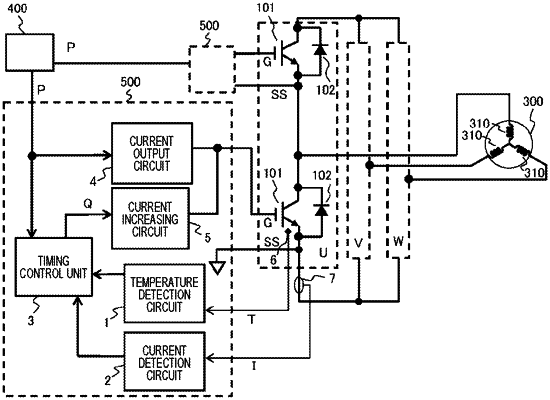
1. A semiconductor element drive device comprising:
a current output circuit that outputs a gate current to a semiconductor element, based on a drive instruction signal for controlling on/off of the semiconductor element;
a current increasing circuit that increases the gate current, based on a delay signal that is outputted after an elapse of a given time from a reference point of time of rising of the drive instruction signal or falling of the drive instruction signal; and
a timing control unit that controls timing of output of the delay signal outputted during a mirror period that is after a point of time at which a current flowing through the semiconductor element reaches a given on-current value and before a point of time at which a voltage between both ends of the semiconductor element reaches a given on-voltage,
wherein the timing control unit controls timing of output of the delay signal, based on at least either a temperature of the semiconductor element or a current flowing through the semiconductor element.
|