| CPC H01Q 9/0457 (2013.01) [H01Q 1/243 (2013.01); H01Q 1/36 (2013.01); H10K 59/00 (2023.02); H10K 59/40 (2023.02)] | 20 Claims |
|
1. An electronic device comprising:
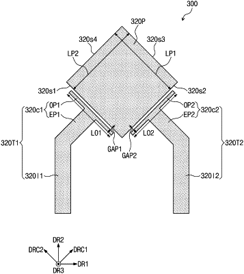
a display panel;
a patch part disposed on the display panel and comprising a first side and a second side;
a first transmission part disposed on the display panel, facing the first side of the patch part, spaced apart from the patch part, and coupled with the patch part; and
a second transmission part disposed on the display panel, facing the second side of the patch part, spaced apart from the patch part, and coupled with the patch part.
wherein the first transmission part is spaced a predetermined gap from the first side, the first transmission part and the patch part are not directly connected, and
wherein the second transmission part is spaced a predetermined gap from the second side, the second transmission part and the patch part are not directly connected.
|