| CPC H01L 29/7849 (2013.01) [H01L 21/823807 (2013.01); H01L 21/823871 (2013.01); H01L 23/481 (2013.01); H01L 27/0924 (2013.01)] | 20 Claims |
|
1. A method for producing a first semiconductor device and a second semiconductor device configured to conduct current through a controlled density of charge carriers in a channel area formed in a semiconductor material, wherein the charge carriers of the first semiconductor device have opposite polarity to the charge carriers of the second semiconductor device, the method comprising the steps of:
producing a stress relaxed buffer (SRB) layer, wherein the back side of the SRB layer is positioned on a substrate;
producing a semiconductor layer on the front side of the SRB layer;
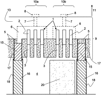
producing the first semiconductor device and the second semiconductor device on the semiconductor layer, wherein the SRB layer is configured to induce a biaxial stress in the channel areas of both devices;
removing the substrate and thinning the SRB layer from its backside;
producing a cavity in the SRB layer from the back side, located underneath the channel area of the second semiconductor device, while no cavity is produced underneath the channel area of the first semiconductor device; and
filling the cavity with one or more materials, thereby creating a stress compensation area, wherein the one or more materials filling the cavity at least partially compensate the biaxial stress in the channel area of the second semiconductor device, and
wherein:
the first semiconductor device and the second semiconductor device are coupled to buried power rails, connected to the back side of the SRB layer by through semiconductor vias (TSVs); or
the SRB layer is a SiGe layer, the semiconductor material is Si, and the compensation area is formed of amorphous silicon or SiN.
|