| CPC H01L 29/7816 (2013.01) [H01L 21/266 (2013.01); H01L 21/26513 (2013.01); H01L 21/308 (2013.01); H01L 21/32139 (2013.01); H01L 29/0653 (2013.01); H01L 29/0865 (2013.01); H01L 29/0882 (2013.01); H01L 29/1087 (2013.01); H01L 29/1095 (2013.01); H01L 29/401 (2013.01); H01L 29/402 (2013.01); H01L 29/4175 (2013.01); H01L 29/41766 (2013.01); H01L 29/66659 (2013.01); H01L 29/66681 (2013.01); H01L 29/7835 (2013.01)] | 12 Claims |
|
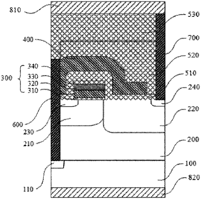
1. A method for manufacturing an LDMOS (laterally diffused metal oxide semiconductor) transistor, comprising:
forming an epitaxial layer having a first doping type on a substrate having said first doping type;
forming a gate structure on an upper surface of said epitaxial layer;
forming a body region having said first doping type and a drift region having a second doping type in said epitaxial layer, and forming a source region having said second doping type in said body region, wherein said second doping type is opposite to said first doping type;
forming a first insulating layer on both said gate structure and an upper surface of said epitaxial layer;
forming a shield conductor layer on said first insulating layer, wherein the shield conductor layer comprises a first vertical portion, a second vertical portion, a first horizontal portion and a second horizontal portion, said first horizontal portion is located between said first vertical portion and said second vertical portion, and is in contact with a first end of said first vertical portion and a first end of said second vertical portion, said second horizontal portion is in contact with a second end of said second vertical portion, said first end of said second vertical portion is opposite to said second end of said second vertical portion; and
forming a first trench, wherein said first trench extends vertically through said first vertical portion of said shield conductor layer, said first insulating layer, said source region, said body region, and said epitaxial layer, to a upper surface of a body contact region in said substrate;
filling said first trench with a conductive material to form a first conductive path,
wherein said first conductive path sequentially passes through said first vertical portion of said shield conductor layer, said first insulating layer, said source region, said body region and said epitaxial layer, to said upper surface of the body contact region in said substrate, to connect said source region with said substrate, and electrically connect said shield conductor layer, said source region and said body contact region, wherein said first vertical portion is in contact with said first conductive path;
wherein said first conductive path is in contact with a side wall of said first insulating layer; and
wherein said source region is isolated from said shield conductor layer by said first insulating layer.
|