US 11,757,016 B2
Semiconductor device and method for fabricating the same
Yi-Fan Li, Tainan (TW); Wen-Yen Huang, Changhua County (TW); Shih-Min Chou, Tainan (TW); Zhen Wu, Kaohsiung (TW); Nien-Ting Ho, Tainan (TW); Chih-Chiang Wu, Tainan (TW); and Ti-Bin Chen, Tainan (TW)
Assigned to UNITED MICROELECTRONICS CORP., Hsin-Chu (TW)
Filed by UNITED MICROELECTRONICS CORP., Hsin-Chu (TW)
Filed on Mar. 30, 2022, as Appl. No. 17/709,385.
Application 16/907,287 is a division of application No. 16/177,368, filed on Oct. 31, 2018, granted, now 10,734,496, issued on Aug. 4, 2020.
Application 17/709,385 is a continuation of application No. 16/907,287, filed on Jun. 21, 2020, granted, now 11,322,598.
Claims priority of application No. 107134933 (TW), filed on Oct. 3, 2018.
Prior Publication US 2022/0223710 A1, Jul. 14, 2022
Int. Cl. H01L 29/49 (2006.01); H01L 29/40 (2006.01); H01L 27/092 (2006.01)
CPC H01L 29/4966 (2013.01) [H01L 27/092 (2013.01); H01L 29/401 (2013.01)] 13 Claims
OG exemplary drawing
 
1. A semiconductor device, comprising:
a substrate having a first region and a second region;
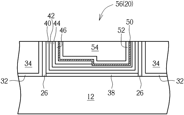
a gate structure on the first region and the second region of the substrate, wherein the gate structure comprises:
a first bottom barrier metal (BBM) layer on the first region and the second region;
a first work function metal (WFM) layer on the first region;
a diffusion barrier layer on the first WFM layer; and
a second WFM layer on a top surface and a sidewall of the diffusion barrier layer.