| CPC H01L 27/14623 (2013.01) [H01L 27/14618 (2013.01); H01L 27/14636 (2013.01); H01L 27/14685 (2013.01); H01L 27/14687 (2013.01); H01L 21/56 (2013.01); H01L 24/95 (2013.01)] | 20 Claims |
|
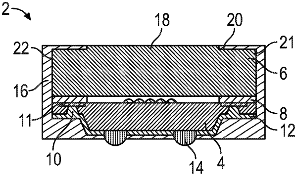
1. A semiconductor package comprising:
a semiconductor die comprising a first side and a second side;
a first side of an optically transmissive lid coupled to the second side of the semiconductor die through one or more dams;
a light block material comprised around the semiconductor package extending from the first side of the semiconductor die to a second side of the optically transmissive lid; and
an opening in the light block material on the second side of the optically transmissive lid that substantially corresponds with an active area of the semiconductor die;
wherein six outer surfaces of the semiconductor package comprise the light block material.
|
|
8. A semiconductor package comprising:
a semiconductor die comprising a first side and a second side;
a first side of an optically transmissive lid coupled to the second side of the semiconductor die through one or more dams; and
a light block material encapsulating the semiconductor package;
wherein the light block material is directly coupled to a second side of the optically transmissive lid opposite the first side of the optically transmissive lid; and
wherein the light block material is directly coupled to the semiconductor die.
|
|
15. A semiconductor package comprising:
a semiconductor die comprising a first side and a second side;
a first side of an optically transmissive lid coupled to the second side of the semiconductor die through one or more dams;
a light block material comprised around the semiconductor package; and
an opening in the light block material on the second side of the optically transmissive lid that substantially corresponds with an active area of the semiconductor die;
wherein the one or more dams are directly coupled to the first side of the optically transmissive lid and the second side of the semiconductor die; and
wherein the light block material is directly coupled to the second side of the optically transmissive lid, the second side of the optically transmissive lid opposite the first side of the optically transmissive lid.
|