| CPC H01L 27/0921 (2013.01) [H01L 21/266 (2013.01); H01L 21/26513 (2013.01); H01L 21/74 (2013.01); H01L 21/823807 (2013.01); H01L 21/823814 (2013.01); H01L 21/823821 (2013.01); H01L 21/823878 (2013.01); H01L 21/823892 (2013.01); H01L 29/0653 (2013.01); H01L 29/0673 (2013.01); H01L 29/0847 (2013.01); H01L 29/1083 (2013.01); H01L 29/42392 (2013.01); H01L 29/66537 (2013.01); H01L 29/66742 (2013.01); H01L 29/66795 (2013.01); H01L 29/7851 (2013.01); H01L 29/78612 (2013.01); H01L 29/78618 (2013.01); H01L 29/78696 (2013.01)] | 20 Claims |
|
1. An integrated circuit, comprising:
a first fin active region and a second fin active region on a semiconductor substrate;
a circuit having a first field-effect transistor (FET) formed on the first fin active region; and
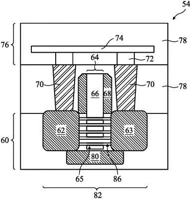
a de-cap device formed on the second fin active region, wherein the de-cap device includes a second FET that further includes
multiple channels vertically stacked on the semiconductor substrate,
a source and a drain, each of the source and the drain extending down to be connected to each of the multiple channels,
a gate stack interposed between the source and the drain, and extended to be around each of the multiple channels, and
a doped feature connecting to the source and drain, wherein
the source and the drain are connected through contact features landing on the source and the drain, respectively,
the doped feature is doped to have a first type conductivity, and
the multiple channels are doped to have a second type of conductivity opposite to the first type conductivity.
|