| CPC H01L 25/0753 (2013.01) [H01L 24/96 (2013.01); H01L 33/62 (2013.01); H01L 33/38 (2013.01); H01L 2224/95101 (2013.01); H01L 2224/95133 (2013.01); H01L 2933/0066 (2013.01)] | 12 Claims |
|
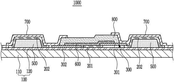
1. A display device comprising:
a substrate;
a pair of electrodes on the substrate, the pair of electrodes comprising a first electrode and a second electrode that are spaced from each other;
a pair of walls between the pair of electrodes and the substrate, the pair of walls comprising a first wall and a second wall that are spaced from each other;
a light emitting element on the pair of electrodes;
an insulating pattern on the light emitting element; and
a pair of contact electrodes overlapping the pair of electrodes, the pair of contact electrodes comprising a first contact electrode and a second contact electrode that are spaced from each other,
wherein the first contact electrode is in contact with a first end of the light emitting element and is electrically connected to the first electrode,
wherein the second contact electrode is in contact with a second end of the light emitting element and is electrically connected to the second electrode,
wherein the first contact electrode is below the insulating pattern, and
wherein at least a portion of the second contact electrode is on the insulating pattern.
|