| CPC H01L 24/80 (2013.01) [H01L 24/08 (2013.01); H01L 2224/0801 (2013.01); H01L 2224/08056 (2013.01); H01L 2224/08059 (2013.01); H01L 2224/08145 (2013.01); H01L 2224/80047 (2013.01); H01L 2224/80095 (2013.01); H01L 2224/80345 (2013.01); H01L 2224/80895 (2013.01); H01L 2224/80896 (2013.01)] | 20 Claims |
|
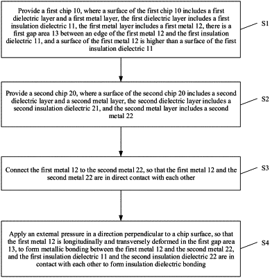
1. A hybrid bonding structure, comprising:
a first chip; and
a second chip, wherein
a surface of the first chip includes a first dielectric layer and a first metal layer, the first dielectric layer includes a first insulation dielectric, the first metal layer includes a first metal, and a first gap area exists between an edge of the first metal and the first insulation dielectric;
a surface of the second chip includes a second dielectric layer and a second metal layer, the second dielectric layer includes a second insulation dielectric, and the second metal layer includes a second metal;
a surface of the first metal is higher than a surface of the first insulation dielectric;
metallic bonding is formed after the first metal is in contact with the second metal, and the first metal is longitudinally and transversely deformed in the first gap area, and
insulation dielectric bonding is formed after the first insulation dielectric is in contact with the second insulation dielectric.
|