US 11,756,887 B2
Backside floating metal for increased capacitance
Nicholas Anthony Lanzillo, Wynantskill, NY (US); Hosadurga Shobha, Niskayuna, NY (US); Huai Huang, Clifton Park, NY (US); and Lawrence A. Clevenger, Saratoga Springs, NY (US)
Assigned to International Business Machines Corporation, Armonk, NY (US)
Filed by International Business Machines Corporation, Armonk, NY (US)
Filed on Jun. 22, 2021, as Appl. No. 17/354,428.
Prior Publication US 2022/0406717 A1, Dec. 22, 2022
Int. Cl. H01L 23/528 (2006.01); H01L 21/768 (2006.01); H01L 23/522 (2006.01); H01L 23/532 (2006.01)
CPC H01L 23/5286 (2013.01) [H01L 21/7684 (2013.01); H01L 23/5223 (2013.01); H01L 23/5226 (2013.01); H01L 23/5283 (2013.01); H01L 23/53209 (2013.01)] 22 Claims
OG exemplary drawing
 
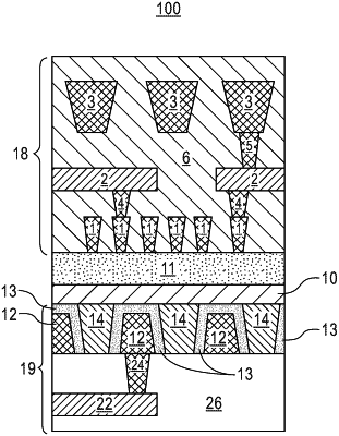
1. A semiconductor structure, the semiconductor structure comprising:
a plurality of portions of a floating metal layer separated by a dielectric material from one or more power and ground lines in one or more backside metal layers on a semiconductor wafer, wherein a height of the plurality of portions of the floating metal layer is less than the height of the one or more power and ground lines.