| CPC H01L 23/5256 (2013.01) [H01L 23/3107 (2013.01); H01L 23/481 (2013.01); H01L 23/4952 (2013.01); H01L 23/49575 (2013.01); H01L 23/5283 (2013.01)] | 39 Claims |
|
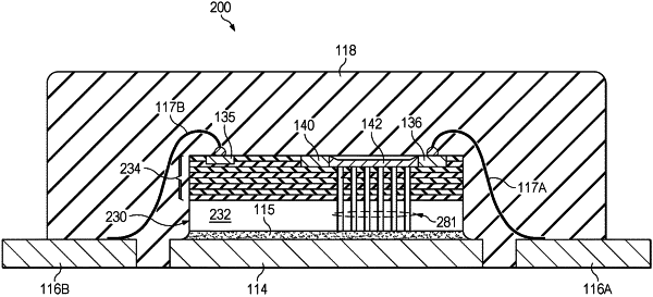
1. A semiconductor package, comprising:
a metallic pad and leads;
a semiconductor die including a semiconductor substrate attached to the metallic pad, and a conductor including a sacrificial fuse element above the semiconductor substrate, the sacrificial fuse element being electrically coupled between one of the leads and at least one terminal of the semiconductor die; and
a multilayer dielectric between the sacrificial fuse element and the semiconductor substrate, the multilayer dielectric forming one or more planar gaps beneath a profile of the sacrificial fuse element.
|