| CPC H01L 23/5226 (2013.01) [H01L 21/76804 (2013.01); H01L 21/76829 (2013.01); H01L 21/76877 (2013.01); H01L 23/5283 (2013.01)] | 20 Claims |
|
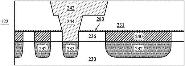
1. A method of forming a semiconductor device comprising:
supplying a substrate comprising two or more first level conductors separated by a third dielectric material;
depositing a first inhibitor in direct contact with the first level conductors, while leaving a portion of a top surface of the third dielectric material exposed;
depositing a fourth dielectric material in contact with the exposed portion of the top surface of the third dielectric material;
depositing a first dielectric material over a surface of the substrate; and
forming a via coupled to one of the first level conductors.
|