| CPC H01L 21/823431 (2013.01) [H01L 29/41791 (2013.01); H01L 29/6681 (2013.01); H01L 29/785 (2013.01)] | 20 Claims |
|
1. A method comprising:
depositing a high-k gate dielectric layer over and along sidewalls of a semiconductor fin;
depositing an n-type work function metal layer over the high-k gate dielectric layer, the n-type work function metal layer comprising aluminum and being deposited to have a same material composition throughout;
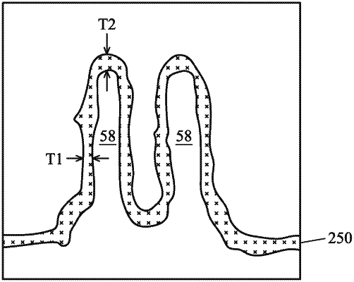
performing a passivation treatment to implant a passivating species into the high-k gate dielectric layer through the n-type work function metal layer, wherein the passivation treatment comprises a remote plasma process, wherein the passivation treatment is directly applied to an aluminum compound of the n-type work function metal layer, wherein the passivation treatment forms a passivated region comprising the passivating species in the high-k gate dielectric layer and the n-type work function metal layer, and wherein a ratio of a first average thickness of the passivated region on the sidewalls of the semiconductor fin to a second average thickness of the passivated region on a top surface of the semiconductor fin is in a range of 0.8:1 to 0.9:1; and
depositing a fill metal over the n-type work function metal layer to form a metal gate stack over the high-k gate dielectric layer, the metal gate stack comprising the n-type work function metal layer and the fill metal.
|