US 11,755,509 B2
Deterministic operation of storage class memory
Frederick A. Ware, Los Altos Hills, CA (US); and Brent Haukness, Sunnyvale, CA (US)
Assigned to Rambus Inc., San Jose, CA (US)
Filed by Rambus Inc., San Jose, CA (US)
Filed on Apr. 7, 2022, as Appl. No. 17/715,404.
Application 17/715,404 is a continuation of application No. 16/660,768, filed on Oct. 22, 2019, granted, now 11,314,669.
Application 16/660,768 is a continuation of application No. 15/376,507, filed on Dec. 12, 2016, granted, now 10,467,157, issued on Nov. 5, 2019.
Claims priority of provisional application 62/268,436, filed on Dec. 16, 2015.
Prior Publication US 2022/0300441 A1, Sep. 22, 2022
This patent is subject to a terminal disclaimer.
Int. Cl. G06F 13/16 (2006.01)
CPC G06F 13/1689 (2013.01) 20 Claims
OG exemplary drawing
 
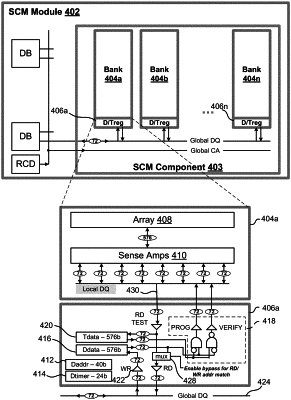
1. A memory device, comprising:
an array of memory cells organized into at least one bank;
a write data register to temporarily store write data associated with a write operation directed to the at least one bank;
a timer register to store a timer value associated with the temporarily stored write data, the timer value representing a predefined write time interval; and
circuitry to selectively provide information relating to the write operation upon expiration of the timer value.