| CPC G02F 1/136286 (2013.01) [G02F 1/1368 (2013.01); G02F 1/134309 (2013.01); G02F 1/136213 (2013.01); G02F 1/136277 (2013.01); G09G 3/3677 (2013.01); H01L 27/124 (2013.01); H01L 27/1225 (2013.01); H01L 27/1255 (2013.01); G02F 1/13606 (2021.01); G02F 1/13629 (2021.01); G02F 1/136295 (2021.01); G02F 2201/123 (2013.01); G02F 2202/10 (2013.01); G02F 2202/103 (2013.01); G09G 2330/021 (2013.01); H01L 29/7869 (2013.01); H01L 29/78669 (2013.01)] | 18 Claims |
|
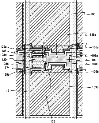
1. A liquid crystal display device comprising a pixel portion, the pixel portion comprising:
a scan line extending in a first direction, the scan line having an opening;
a capacitor wiring extending in parallel to the first direction, the capacitor wiring comprising same materials of the scan line;
a signal line extending in parallel to a second direction intersecting with the first direction, the signal line having a portion overlapping with the opening of the scan line;
a conductive layer comprising same materials of the signal line;
a transistor comprising a semiconductor film electrically connected to the signal line and the conductive layer; and
a capacitor provided in an area where the capacitor wiring and the conductive layer overlap,
wherein the semiconductor film comprises amorphous silicon,
wherein in the top view, the scan line comprises a branch part having a first portion and a second portion sandwiching the opening and a first region being adjacent to the branch part and extending in the first direction with a first width in the second direction,
wherein a sum of a width of the branch part in the second direction and a width of the opening in the second direction is larger than the first width,
wherein in the top view, the capacitor wiring comprises a second region extending in parallel to the first direction with a second width in the second direction and a third region projected from a first part of the second region to only one side in the second direction, and
wherein in the top view, the conductive layer overlaps with the first part of the second region and the third region of the capacitor wiring.
|