| CPC H10K 85/633 (2023.02) [C07C 211/54 (2013.01); C07C 211/61 (2013.01); C07D 209/88 (2013.01); C07D 307/91 (2013.01); C07D 333/76 (2013.01); H10K 50/156 (2023.02); H10K 50/818 (2023.02); H10K 50/828 (2023.02); H10K 50/858 (2023.02); H10K 85/636 (2023.02); C07C 2601/14 (2017.05); C07C 2603/18 (2017.05); C07C 2603/74 (2017.05); H10K 85/615 (2023.02); H10K 85/626 (2023.02); H10K 85/6572 (2023.02); H10K 85/6574 (2023.02); H10K 85/6576 (2023.02); H10K 2102/3026 (2023.02); H10K 2102/351 (2023.02)] | 26 Claims |
|
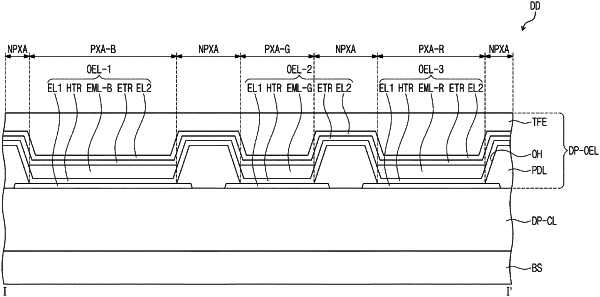
1. A light emitting diode, comprising:
a first electrode;
a hole transport region disposed on the first electrode;
an emission layer disposed on the hole transport region;
an electron transport region disposed on the emission layer; and
a second electrode disposed on the electron transport region,
wherein the hole transport region comprises:
a first hole transport layer disposed adjacent to the first electrode, the first hole transport layer having a first refractive index;
a second hole transport layer disposed adjacent to the emission layer, the second hole transport layer having a second refractive index; and
a third hole transport layer disposed between the first hole transport layer and the second hole transport layer, the third hole transport layer having a third refractive index which is greater than each of the first refractive index and the second refractive index.
|