| CPC H10K 59/38 (2023.02) [H10K 50/156 (2023.02); H10K 50/813 (2023.02); H10K 50/816 (2023.02); H10K 50/822 (2023.02); H10K 59/12 (2023.02); H10K 59/353 (2023.02); H10K 71/00 (2023.02)] | 18 Claims |
|
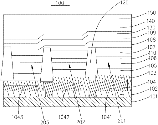
1. An organic light-emitting diode device comprising:
a substrate;
a first electrode layer, wherein the first electrode layer is one of an anode layer or a cathode layer, and the first electrode layer comprises a first sub-electrode layer disposed on the substrate and a second sub-electrode layer electrically connected with the first sub-electrode layer;
a color filter layer disposed on a side of the second sub-electrode layer close to the substrate;
a light emitting layer;
a second electrode layer, wherein the second electrode layer is the other of the anode layer or the cathode layer, and the light emitting layer is disposed between the second electrode layer and the second sub-electrode layer of the first electrode layer; and
a pixel defining layer extending from the second sub-electrode layer in a direction away from the substrate, located below the second electrode layer; and defining light emitting regions of sub-pixels,
wherein the color filter layer is configured to adjust a light emitted by the light emitting layer; and
wherein an orthographic projection of the pixel defining layer on the substrate overlaps with an orthographic projection of the color filter layer on the substrate.
|