| CPC H10K 59/1216 (2023.02) [H04N 9/30 (2013.01); H10K 59/126 (2023.02); H10K 59/131 (2023.02); H10K 71/00 (2023.02); H10K 59/1201 (2023.02)] | 20 Claims |
|
1. A display substrate, comprising:
a base substrate; and
an array of sub-pixels on the base substrate;
wherein each sub-pixel includes:
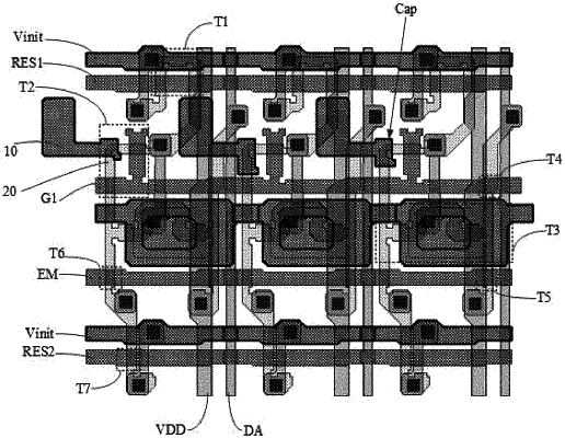
a power signal line; wherein at least part of the power signal line extends along a first direction;
sub-pixel driver circuits; wherein each sub-pixel driver circuit includes a driver transistor and a compensation transistor of double-gate structure; a first terminal of the driver transistor is electrically coupled with the power signal line; a first terminal of the compensation transistor of double-gate structure is electrically coupled with a second terminal of the driver transistor; a second terminal of the compensation transistor of double-gate structure is electrically coupled with a gate of the driver transistor; an active layer of the compensation transistor of double-gate structure includes a first semiconductor pattern, a second semiconductor pattern, and a conductor pattern located between the first semiconductor pattern and the second semiconductor pattern;
a shielding pattern electrically coupled with the power signal line in the sub-pixel which is adjacent the shielding pattern in a second direction; wherein there is an overlap area between an orthographic projection of the shielding pattern onto the base substrate and an orthographic projection of the conductor pattern onto the base substrate; the second direction intersects the first direction;
wherein the array of sub-pixels include multiple first sub-pixels and multiple second sub-pixels; the overlap area in the first sub-pixel is greater than the overlap area in the second sub-pixel.
|