| CPC H10K 59/1213 (2023.02) [H01L 27/1225 (2013.01); H01L 27/1251 (2013.01); H01L 27/1255 (2013.01); H01L 27/1259 (2013.01); H10K 59/1216 (2023.02); H10K 59/131 (2023.02); H01L 27/0688 (2013.01); H01L 27/124 (2013.01); H01L 27/1222 (2013.01); H01L 27/1262 (2013.01); H01L 29/66757 (2013.01); H01L 29/66969 (2013.01); H01L 29/7869 (2013.01); H01L 29/78675 (2013.01); H10K 59/1201 (2023.02)] | 5 Claims |
|
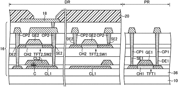
1. A display device comprising:
a pixel electrode that is provided in a display region configured to display an image;
a common electrode that is disposed above the pixel electrode;
a light-emitting element layer that is interposed between the pixel electrode and the common electrode;
a first thin film transistor including a first gate electrode coupled to the pixel electrode in the display region, no other transistor being coupled between the first thin film transistor and the pixel electrode;
a first conductive layer that is provided under and overlaps with the first thin film transistor;
a circuit layer that is provided in a peripheral region outside the display region; and
a second thin film transistor including a second gate electrode in the circuit layer,
wherein a first channel of the first thin film transistor is made of an oxide semiconductor, and the second thin film transistor is positioned at a lower layer in comparison with the first thin film transistor, and the second gate electrode is in the same layer as the first conductive layer.
|