| CPC H10K 59/1213 (2023.02) [H01L 29/045 (2013.01); H01L 29/1604 (2013.01); H01L 29/78675 (2013.01); H10K 50/12 (2023.02); H10K 50/165 (2023.02); H10K 59/123 (2023.02); H10K 71/00 (2023.02)] | 13 Claims |
|
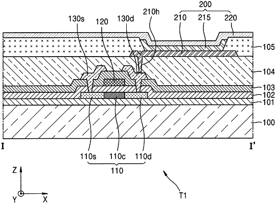
1. A display apparatus, comprising:
a substrate;
a first thin film transistor on the substrate, the first thin film transistor including an active layer including a source region, a drain region, and a channel region between the source region and the drain region; and
a display device on the substrate and electrically connected to the first thin film transistor, wherein
the source region, the drain region, and the channel region include a first dopant and a second dopant, the second dopant being different from the first dopant, and
a concentration of the first dopant in the channel region is less than a concentration of the first dopant in the source region and the drain region.
|