| CPC H10K 50/115 (2023.02) [H10K 50/13 (2023.02); H10K 71/00 (2023.02); H10K 71/15 (2023.02); H10K 71/441 (2023.02); H10K 2101/30 (2023.02); H10K 2102/351 (2023.02)] | 24 Claims |
|
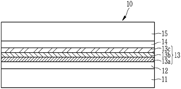
1. A light emitting device, comprising
a first electrode and a second electrode facing each other, and an emission layer disposed between the first electrode and the second electrode, and comprising quantum dots,
a first charge auxiliary layer disposed between the emission layer and the first electrode, and a second charge auxiliary layer disposed between the emission layer and the second electrode,
wherein the emission layer comprises a plurality of layers comprising quantum dots, and
the quantum dots comprise an organic ligand on a surface, and a content of the organic ligand of the quantum dots increases sequentially from a first layer in contact with the first charge auxiliary layer to a second layer in contact with the second charge auxiliary layer.
|