| CPC H10B 63/30 (2023.02) [G11C 13/0002 (2013.01); G11C 13/0021 (2013.01); H10N 70/20 (2023.02); H10N 70/231 (2023.02)] | 20 Claims |
|
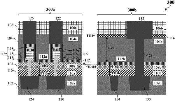
1. A semiconductor device comprising:
a first insulating layer;
a second insulating layer arranged over the first insulating layer;
a further insulating layer under the first insulating layer;
a base layer under the further insulating layer;
a memory structure arranged within a memory region and comprising a resistance changing memory element within the first insulating layer; and
a logic structure arranged within a logic region;
wherein in the memory region, the first insulating layer contacts the second insulating layer and wherein in the logic region, the semiconductor device further comprises a stop layer arranged between the first insulating layer and the second insulating layer,
wherein a top surface of the first insulating layer that contacts the second insulating layer in the memory region and a top surface of the stop layer that contacts the second insulating layer in the logic region are each the same distance away from a top surface of the base layer.
|