| CPC H10B 12/482 (2023.02) [H01L 21/71 (2013.01); H01L 29/40114 (2019.08); H01L 29/7926 (2013.01); H10B 12/053 (2023.02); H10B 12/31 (2023.02); H10B 12/315 (2023.02); H10B 12/34 (2023.02); H10B 12/48 (2023.02); H01L 21/823475 (2013.01)] | 22 Claims |
|
1. A method of forming a volatile memory device, the method comprising:
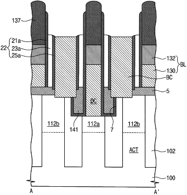
forming a bit line structure having a vertical sidewall protruding from a substrate;
forming a lower spacer layer on the vertical sidewall to have a first thickness;
removing the lower spacer layer from the substrate adjacent to the bit line structure to form a lower spacer having the first thickness from the vertical sidewall to an outer sidewall of the lower spacer;
forming a storage node contact plug on the substrate aligned to the lower spacer to cover the outer sidewall of the lower spacer and to expose an upper portion of the lower spacer;
removing the upper portion of the lower spacer using the storage node contact plug as a mask; and
forming an upper spacer on the vertical sidewall to expose an uppermost portion of the outer sidewall of the lower spacer, the upper spacer formed to have a second thickness that is less than the first thickness,
wherein the upper spacer extends in a vertical direction, and a bottom-most surface of the upper spacer is offset above an uppermost surface of the storage node contact plug, such that the bottom-most surface of the upper spacer does not abut the uppermost surface of the storage node contact plug.
|