| CPC H04L 12/12 (2013.01) [G06F 1/26 (2013.01); G06F 1/32 (2013.01); G06F 1/325 (2013.01); G06F 1/3209 (2013.01); G06F 15/17 (2013.01); H04L 12/64 (2013.01); H04N 21/43637 (2013.01); H04N 21/4436 (2013.01); H04N 21/6377 (2013.01); H04W 52/0251 (2013.01); H04W 52/0274 (2013.01); H04W 52/287 (2013.01); H04W 52/0248 (2013.01); H04W 84/12 (2013.01); H04W 88/06 (2013.01); Y02D 30/70 (2020.08)] | 18 Claims |
|
1. An electronic device, comprising:
a communication circuit including a first circuit and a second circuit;
at least one processor electrically or operatively connected to the communication circuit; and
a memory electrically or operatively connected to the at least one processor,
wherein, the memory stores instructions which, when executed by the at least one processor, are configured to cause the at least one processor to perform operations comprising:
controlling the first circuit to perform first communication through a first channel of a first baseband and second communication through a second channel of the first baseband;
changing the second channel of the first baseband to a third channel of a second baseband based on controlling the second circuit to perform the second communication through the third channel of the second baseband;
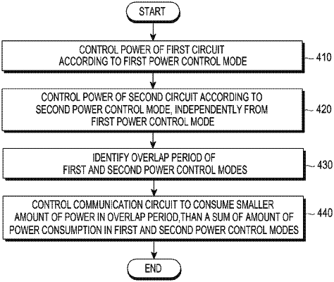
when the first communication by the first circuit and the second communication by the second circuit are performed through the first channel of the first baseband and the third channel of the second baseband, respectively, controlling the first circuit to operate according to a first power control mode associated with the first communication, and controlling the second circuit to operate according to a second power control mode associated with the second communication;
identifying a first sleep period during which the first circuit operates in a sleep mode in response to operating in the first power control mode, and identifying a second sleep period during which the second circuit operates in the sleep mode in response to operating in the second power control mode;
identifying an overlap period in which the first sleep period and the second sleep period coincide; and
during the overlap period, controlling the communication circuit to operate in a deep sleep mode with power that is less than or equal to a predetermined power.
|