| CPC H03K 17/04123 (2013.01) | 19 Claims |
|
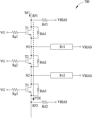
1. A switch device comprising:
a first radio-frequency (RF) terminal, configured to receive an RF signal and coupled to a bias voltage terminal, wherein the bias voltage terminal provides a bias voltage;
a second RF terminal, configured to receive the RF signal through a predetermined path and coupled to the bias voltage terminal, wherein the predetermined path is between the first RF terminal and the second RF terminal;
a first transistor, comprising a first terminal coupled to the first RF terminal, a second terminal, and a control terminal;
a second transistor, comprising a first terminal coupled to the second terminal of the first transistor, a second terminal coupled to the second RF terminal, and a control terminal;
a first variable resistance element, comprising a first terminal coupled to the second terminal of the first transistor, and a second terminal coupled to the bias voltage terminal;
a third transistor coupled between the second transistor and the second RF terminal, wherein the third transistor comprises a first terminal coupled to the second terminal of the second transistor, a second terminal coupled to the second RF terminal, and a control terminal configured to receive a first control signal; and
a second variable resistance element comprising a first terminal coupled to the second terminal of the second transistor, and a second terminal coupled to the bias voltage terminal;
wherein:
the first variable resistance element provides a first resistance when the first transistor and the second transistor are in a transient state according to the first control signal;
the first variable resistance element provides a second resistance when the first transistor and the second transistor are in an ON state according to the first control signal, and the second resistance is larger than the first resistance; and
the third transistor is in an ON state, an OFF state, or a transient state according to the first control signal.
|