| CPC H02M 3/33592 (2013.01) [H02M 1/083 (2013.01); H02M 3/33571 (2021.05); H02M 1/007 (2021.05); H02M 1/008 (2021.05); H02M 1/0058 (2021.05); H02M 3/01 (2021.05); H02M 3/158 (2013.01); H02M 3/1582 (2013.01); H02M 3/33546 (2013.01); H02M 3/33561 (2013.01); H02M 3/33576 (2013.01); H02M 3/33584 (2013.01); Y02B 70/10 (2013.01)] | 24 Claims |
|
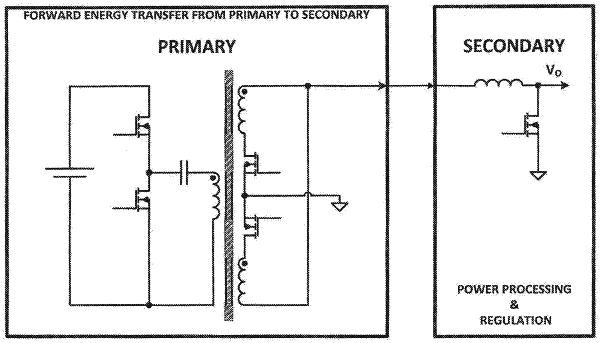
1. A two-transistor forward switching cell comprising:
two primary switching elements connected between an input voltage source and a primary winding of a transformer, wherein the input voltage source has two terminations and the primary winding has opposite ends;
the primary switching elements are connected to the primary winding at the opposite ends thereof;
reset diodes, wherein one of the reset diodes is connected between one of the opposite ends of the primary winding and one of the terminations of the input voltage source, and the other of the reset diodes is connected between another of the opposite ends of the primary winding and another of the terminations of the input voltage source;
two synchronous rectifiers, defined as main synchronous rectifiers, each having a source and a drain;
wherein the transformer includes at least a secondary winding connected to the drains of the synchronous rectifiers;
one of the synchronous rectifiers is defined as a forward rectifier and is on during at least a portion of a time when the two primary switching elements are on, and the other of the synchronous rectifiers is defined as freewheeling rectifier and is off during the time when the two primary switching elements are on;
wherein the freewheeling rectifier is connected to at least one controlled current source; and
wherein the two synchronous rectifiers are both on for a common predetermined time;
the at least one controlled current source comprises an inductive element connected to the freewheeling rectifier and to a switching node, referred to as secondary switching node, which is a common connection of first and second additional synchronous rectifiers connected in a totem pole configuration and placed across an output capacitor and a load;
the output capacitor is connected in parallel to the load;
the first additional synchronous rectifier, defined as a boost switch, is connected to a freewheeling rectifier terminal which is not connected to the inductive element, and the second additional synchronous rectifier, defined as a diode switch, is connected to the output capacitor and the load; and
the boost switch is on during at least a portion of a time when the two primary switching elements are on, and the diode switch turns on after the boost switch turns off and is on until a current through the inductive element reaches zero or slightly negative such that when the freewheeling rectifier turns off, a magnetizing current and a negative portion of a current flowing through the diode switch is transferred to the primary winding, thereby discharging a parasitic capacitance reflected across the primary switching elements to a predetermined voltage level.
|