| CPC H01Q 21/0025 (2013.01) [H01Q 1/2283 (2013.01); H01Q 1/243 (2013.01); H01Q 21/064 (2013.01)] | 20 Claims |
|
1. An antenna module comprising:
a communication circuit;
an antenna part comprising multiple antenna elements constituting a subarray; and
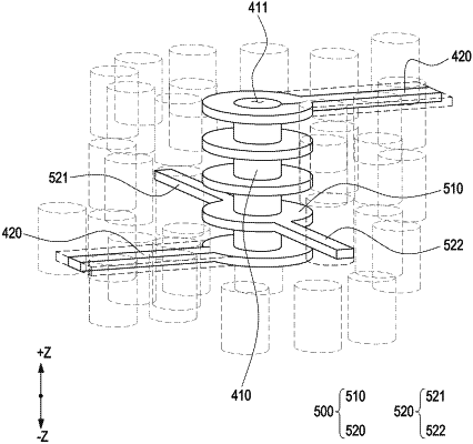
a network part disposed beneath the antenna part in multiple layers, the network part comprising at least one transmission line configured to be branched to positions of the multiple antenna elements, a via hole extending through the multiple layers, and a stub structure disposed in an area adjacent to the via hole,
wherein an open stub structure designed on a first layer configured to form a ground plane, among the multiple layers, comprises:
a first via pad disposed adjacent to the via hole,
a first open stub extending from the first via pad in a first direction, and
a first slot part formed to surround an edge of the first via pad and the first open stub, and
wherein a short stub structure designed on a second layer different from the first layer comprises:
a second via pad disposed adjacent to the via hole,
a short stub extending from the second via pad in a second direction,
a transformer extending from the second via pad in a third direction different from the second direction and connected to the at least one transmission line, and
a second slot part formed to surround at least a portion of an edge of the second via pad, the short stub, and the transformer.
|