| CPC H01L 33/504 (2013.01) [H01L 25/0753 (2013.01); H01L 33/44 (2013.01); H01L 33/505 (2013.01); H01L 33/62 (2013.01); H01L 2933/0041 (2013.01)] | 14 Claims |
|
1. A method for manufacturing a display device, the method comprising:
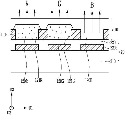
providing a light emitting element layer including a plurality of light emitting elements, on a substrate;
providing a first photosensitive resin layer on the light emitting element layer;
providing a passivation layer between the light emitting element layer and the first photosensitive resin layer;
driving a plurality of first light emitting elements among the plurality of light emitting elements, the driving of the plurality of first light emitting elements hardening a portion of the first photosensitive resin layer which corresponds to the plurality of first light emitting elements and faces the plurality of first light emitting elements with the passivation layer therebetween; and
providing on the plurality of first light emitting elements and the passivation layer, a plurality of first color converting patterns as the portion of the first photosensitive resin layer which is hardened, by removing a remaining portion of the first photosensitive resin layer except for the portion of the first photosensitive resin layer which is hardened.
|