| CPC H01L 31/0543 (2014.12) [H01L 31/0481 (2013.01); H01L 31/1868 (2013.01); Y02E 10/50 (2013.01)] | 20 Claims |
|
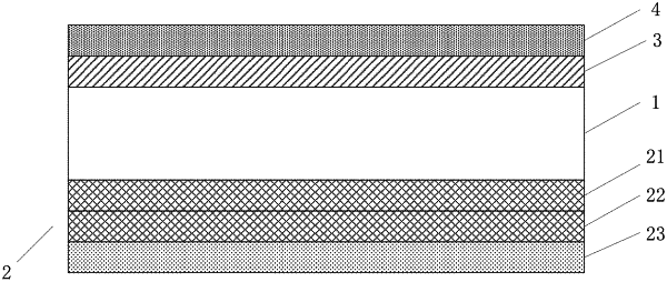
1. A solar cell, comprising:
a semiconductor layer having a resistivity ranging from 0.5 Ω·cm to 3.5 Ω·cm;
a diffusion layer formed on a front surface of the semiconductor layer, wherein the diffusion layer and the semiconductor layer form a PN junction;
a front passivation layer formed on the diffusion layer; and
a passivation film stack provided on a back surface of the semiconductor layer,
wherein the passivation film stack comprises at least one silicon oxynitride film layer and at least one silicon nitride film, a sum of thicknesses of layers of the passivation film stack is in a range from 160 nm to 260 nm, the at least one silicon oxynitride film layer has a thickness ranging from 90 nm to 150 nm, and the at least one silicon oxynitride film layer includes a silicon-rich silicon oxynitride film having a silicon atom concentration ranging from 5×10²¹/cm3 to 2.5×10²²/cm3.
|